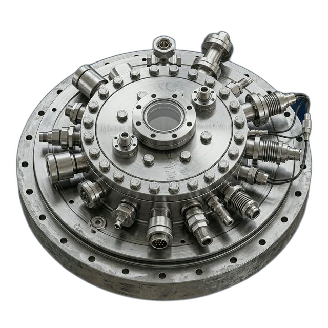
Electrostatic Chuck Base Plate — 6061-T6 Aluminum for Plasma Etch
An etch equipment company developing a new ESC (electrostatic chuck) assembly needed a base plate that serves as the thermal management foundation. It contains helium cooling channels that maintain wafer temperature uniformity during plasma etch — temperature non-uniformity across the wafer causes etch rate variation and kills device yield.
The Challenge
Helium cooling channels (3mm wide × 4mm deep) routed in a spiral pattern across a 300mm disk. Channel floor flatness must hold ±0.0005″ to ensure uniform helium flow. Top surface flatness 0.0003″ for bonding to the ceramic ESC layer. 15 lift pin bores at ±0.001″ true position — if any bore is off, lift pins can scratch or crack the wafer.
Our Approach
Channels machined with a 3mm endmill in a continuous spiral toolpath — no plunge-in/retract marks that would disrupt helium flow. Top surface diamond-fly-cut for sub-micron flatness. Lift pin bores drilled and reamed in the final operation after all material removal is complete. Ultra-clean processing: semiconductor-grade DI water rinse, nitrogen dry, double-bagged.
The Result
Top surface flatness measured 0.0002″ — beating the 0.0003″ spec. Channel depth uniformity ±0.0003″. The customer reported the best wafer temperature uniformity (±0.3°C) of any base plate they’ve tested from any vendor.
Why the ESC Base Plate Is the Foundation of Etch Uniformity
In a plasma etch tool, the electrostatic chuck holds the wafer in place using electrostatic force generated by electrodes embedded in a ceramic puck. But the ceramic puck sits on an aluminum base plate, and it’s the base plate that does the actual thermal management. Helium gas flows through channels machined into the top of the base plate, passes through the bonding layer, and creates a thin gas cushion between the ceramic and the wafer. This helium backside cooling is what keeps the wafer at a uniform temperature while the plasma bombards it with ions.
If the helium channels are not uniform in depth, the gas flow varies across the wafer. More flow in one zone means more cooling; less flow means less cooling. A temperature variation of even 1°C across a 300mm wafer can cause measurable etch rate non-uniformity — deep enough to affect critical dimension control on advanced-node devices. The base plate isn’t glamorous, but it directly determines whether the etch tool can hold spec.
The Precision Stack-Up Problem
The base plate participates in a precision stack-up that starts at the aluminum surface and ends at the wafer. The top surface of the base plate must be flat enough to bond uniformly to the ceramic ESC puck. Any gap in the bond layer creates a thermal resistance hot spot. The channels must be uniform in depth so that helium flow — and therefore cooling — is even. The lift pin bores must be positioned accurately so that the pins don’t contact the wafer edge during loading, which would chip or crack the wafer.
The material is 6061-T6 aluminum, chosen for its high thermal conductivity (167 W/m·K) and machinability. But 6061-T6 machines almost too easily — it’s prone to built-up edge on cutting tools, which creates surface finish variations and can leave embedded aluminum particles in the channel floors. Those particles can break free during helium flow and migrate to the wafer backside, causing contamination.
How We Solved It
Every aspect of this part required a different machining strategy, and the sequence of operations mattered as much as the individual cuts:
- Continuous spiral toolpath for helium channels. Most shops would program the spiral channels as a series of linear moves with arc interpolations. We used a true spiral toolpath that keeps the 3mm endmill in continuous contact with the material — no plunge points, no retract points, no transition marks. Every interruption in the cut leaves a witness mark on the channel floor that disrupts laminar helium flow. Our continuous path eliminated all toolpath artifacts.
- Diamond fly-cutting for bonding surface. The top surface flatness requirement of 0.0003″ across a 300mm disk is beyond what conventional face milling can reliably achieve. We diamond-fly-cut the surface — a single-point natural diamond tool mounted on a precision fly-cutting head. The diamond produces a mirror-like surface with sub-micron flatness and virtually zero subsurface damage, which is critical for adhesive bonding to the ceramic ESC puck.
- Lift pin bores machined last. Internal stress redistribution during material removal can shift bore positions by several tenths. We drilled and reamed all 15 lift pin bores in the final operation, after the channels and top surface were complete. By this point, virtually all material removal was done and the stress state was stable. Every bore was measured on the CMM and all 15 were within ±0.0008″ true position — comfortably within the ±0.001″ spec.
- Ultra-clean semiconductor processing. After machining, every base plate was cleaned with semiconductor-grade DI water to remove all cutting fluid residue and aluminum particles. Parts were dried with filtered nitrogen and double-bagged in cleanroom packaging. We verified particle counts on each part — zero particles >0.5μm on any bonding or channel surface.
Thermal Performance Results
The customer bonded their ceramic ESC pucks to all three base plates and installed them in their etch tools for thermal qualification. Using embedded thermocouples and wafer-level temperature mapping, they measured wafer temperature uniformity at ±0.3°C during plasma etch — the tightest uniformity they had achieved with any base plate from any vendor. They attributed the improvement to two factors: the consistent channel depth (uniform helium flow) and the superior bonding surface flatness (no thermal resistance hot spots in the adhesive layer).
The lift pin performance was equally clean — zero wafer edge chips or cracks during the 500-wafer qualification run. The customer confirmed that pin-to-wafer alignment was within their optical verification spec at all 15 locations.
What the Customer Said
“Temperature uniformity is the single most important parameter in our etch tool, and it starts at the base plate. RivCut’s channel depth consistency and bonding surface flatness gave us the best thermal data we’ve seen. We’re qualifying these base plates as our production standard.”
By the Numbers
Upload Your CAD File
Get instant AI pricing, a free DFM review, and full documentation on every order.
No minimums · 100% Made in USA · Never brokered · Ships anywhere in the US